Wells Gardner 6100 vector deflection #2
This deflection board had come to me with most of the transistors replaced, but gave the following sharply distorted picture:
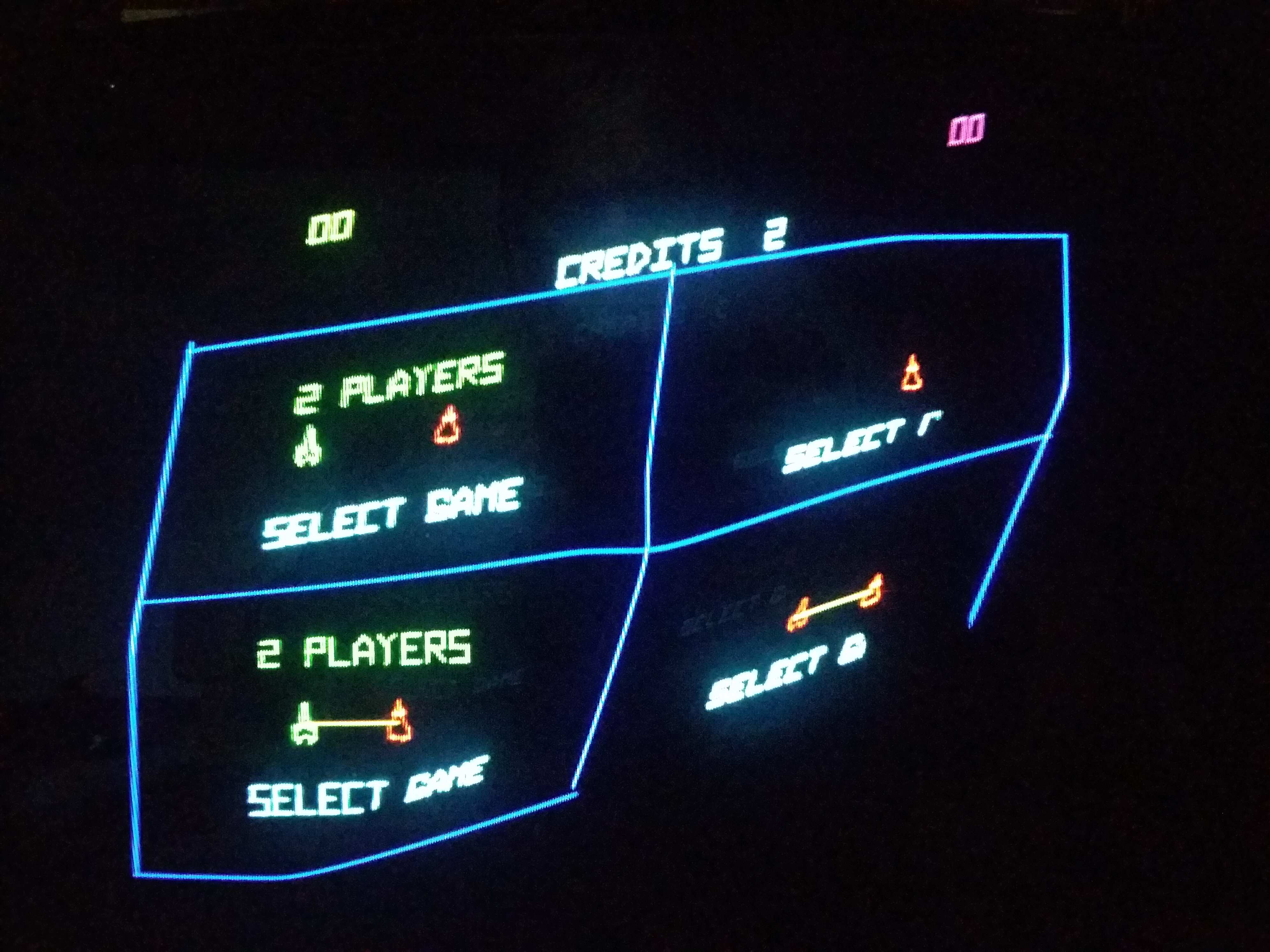
To me this says that the actual high power deflection parts were working OK, but the input X and Y signals themselves were being distorted.
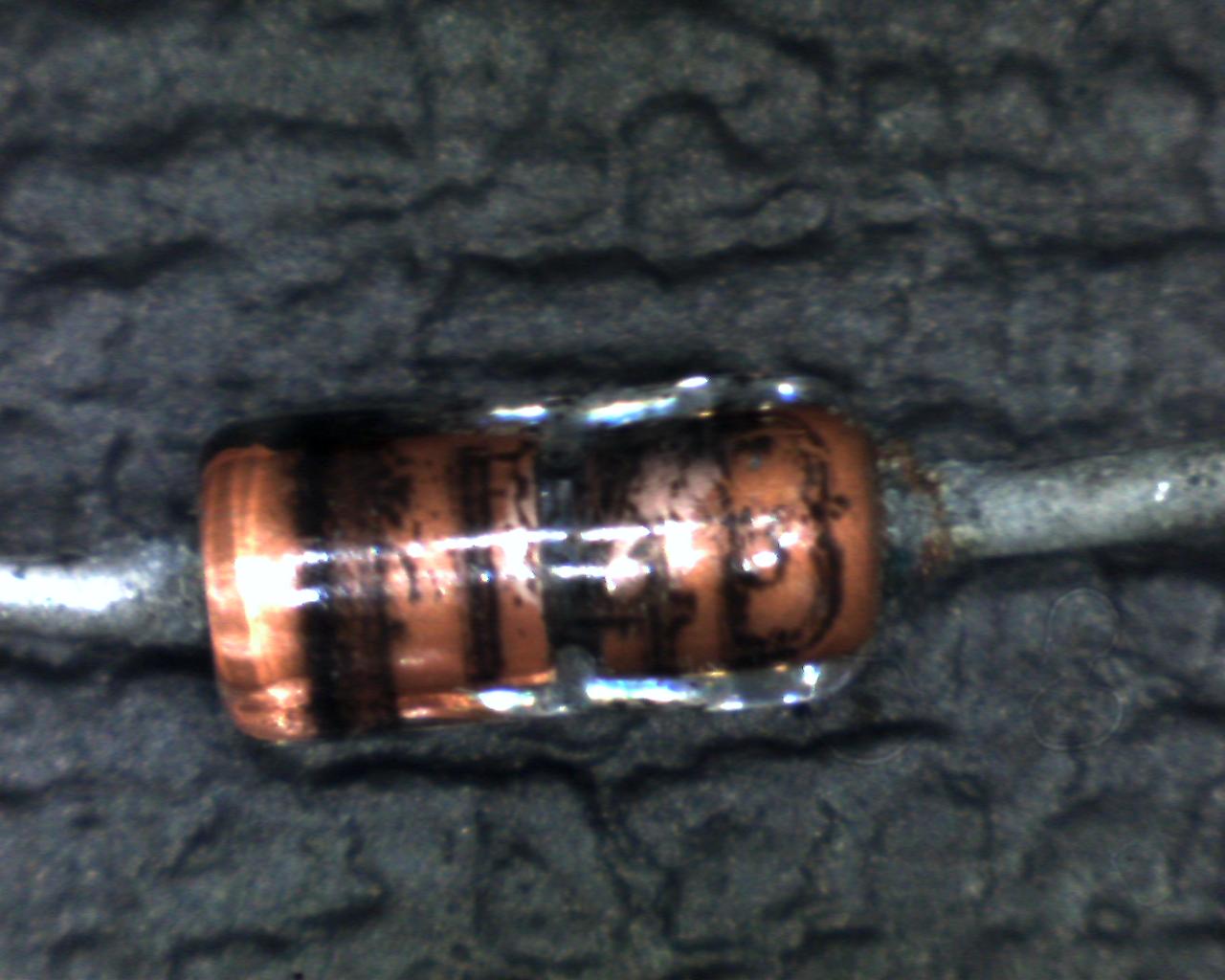
This is a P327 revision PCB, which has some extra clamping circuitry on the inputs to help prevent failures from too high a signal voltage. This circutry has some 1N914 diodes in it, and as I tested some with a meter diode test I found one that read a high forward voltage drop. I desoldered it from the board in case other parts of the circuit were affecting the meter reading, but no it still read as about 1.5V rather than the expected about 0.6V for a silicon diode.
The real surprise to me was that it wasn't just a single 1N914 that was reading high, but a total of 5.
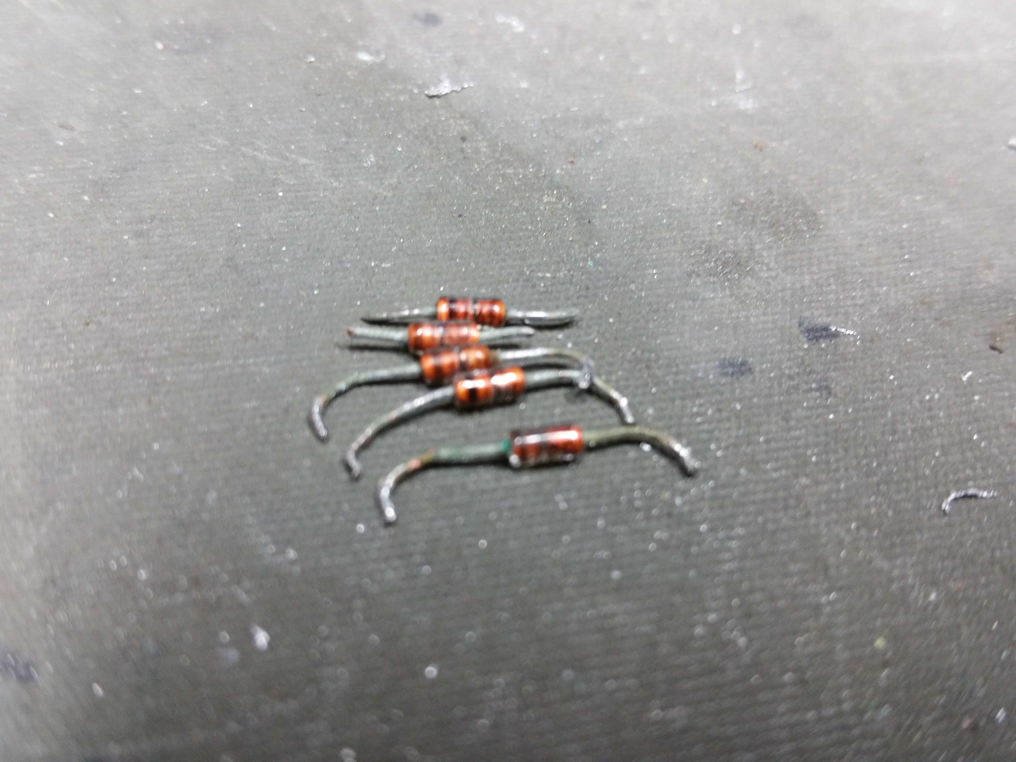
Some read much higher forward voltages.

None of the diodes are particularly stressed in this circuit, unlike the larger transistors that often fail on 6100's. Maybe a bad batch of diodes from manufacture? Some sort of atmospheric corrosion, like salt in the air near the seaside arcades? A noxious fart nearby from a previous owner, that only attacked 1N914 diodes???
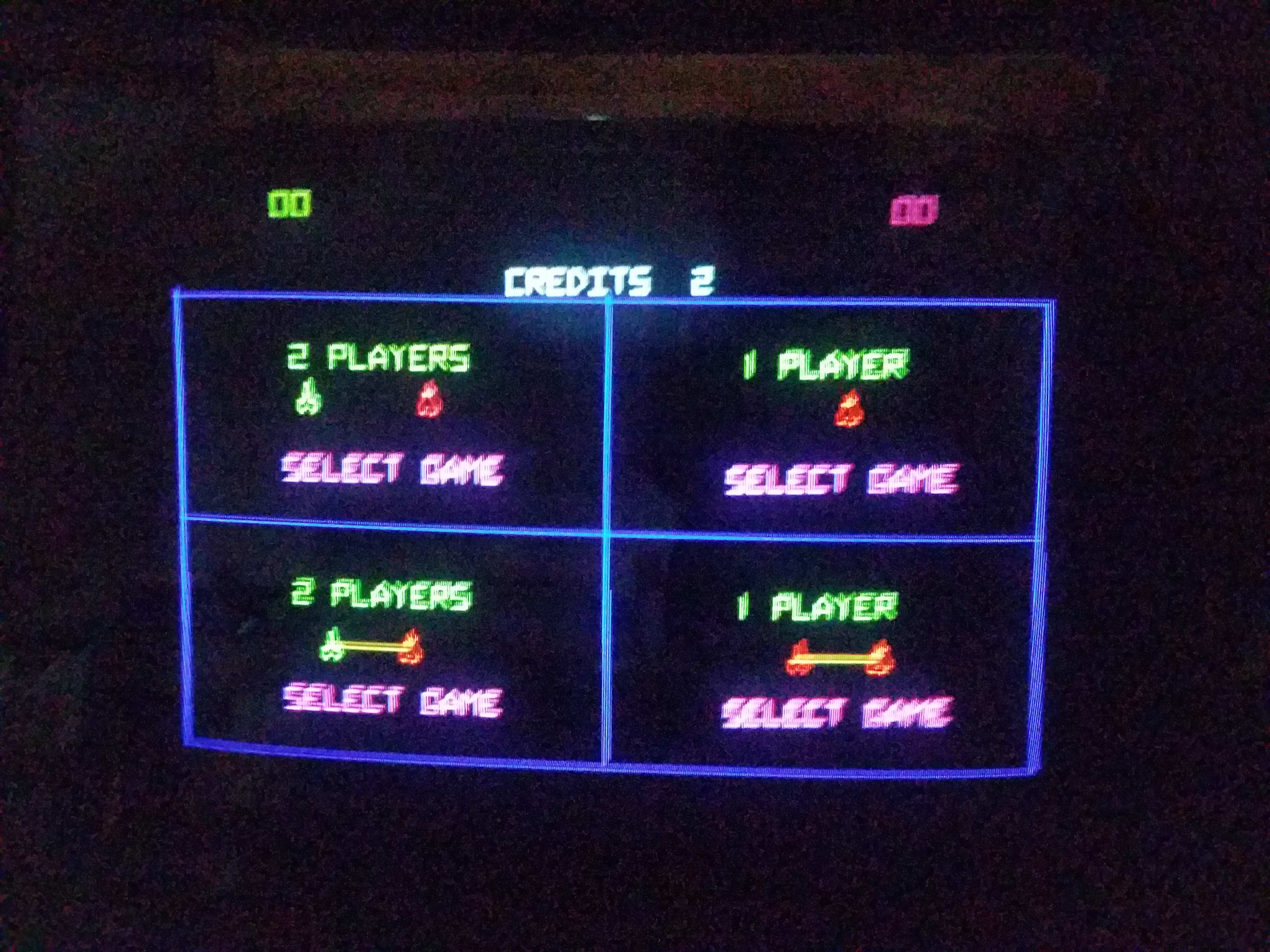
Replacing the failed diodes restored the picture to normal operation.
This deflection board had come to me with most of the transistors replaced, but gave the following sharply distorted picture:
To me this says that the actual high power deflection parts were working OK, but the input X and Y signals themselves were being distorted.
This is a P327 revision PCB, which has some extra clamping circuitry on the inputs to help prevent failures from too high a signal voltage. This circutry has some 1N914 diodes in it, and as I tested some with a meter diode test I found one that read a high forward voltage drop. I desoldered it from the board in case other parts of the circuit were affecting the meter reading, but no it still read as about 1.5V rather than the expected about 0.6V for a silicon diode.
The real surprise to me was that it wasn't just a single 1N914 that was reading high, but a total of 5.
Some read much higher forward voltages.
None of the diodes are particularly stressed in this circuit, unlike the larger transistors that often fail on 6100's. Maybe a bad batch of diodes from manufacture? Some sort of atmospheric corrosion, like salt in the air near the seaside arcades? A noxious fart nearby from a previous owner, that only attacked 1N914 diodes???
Replacing the failed diodes restored the picture to normal operation.