Juno First Boot Leg

NivagSwerdna

Active member
Feedback
1 (100%)
Credits
817CR
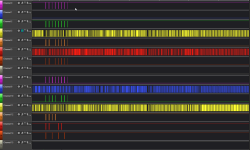
So as a parting gesture before bedtime I decided to look at what was happening at one of the 7489s...


1728761770052.png
The pins are numbered 1, 2, 3... channels 0, 1, 2... you get the drift.
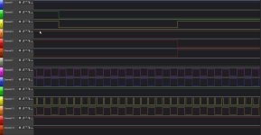
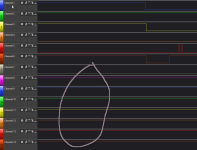
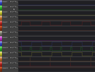
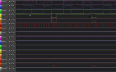
I think this shows that the load into the 64bit RAM is working nicely... You can see nWE being pulsed eight times and the address (ch 12,13,14) going 7,6,5,4,3,2,1,0... so that looks good. There is a complete absence of the address pulsing when it is meant to be read back out... I think that suggests I need to swim upstream to the LS157...
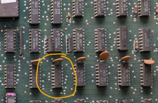
JFVideoGen1c.png

but that's a job for tomorrow. zzzZZZZZZZ
 

NivagSwerdna

Active member
Feedback
1 (100%)
Credits
817CR
As a bedtime story...

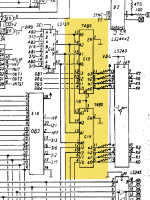
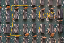
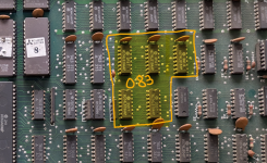
We are heading towards what would be the Konami 083 custom but we don't have one... however I spy with my little eye... 4x 74LS194 and a 74LS157... I haven't buzzed this out but I bet you that's the 083 equivalent...
1728762940525.png
and if you don't believe me look at the attached schematic which I made a while back when I was looking at other boards...

Sweet dreams.
 

Attachments

  • RSTU_K083_v1_0.pdf
    128.4 KB · Views: 13

NivagSwerdna

Active member
Feedback
1 (100%)
Credits
817CR
Ok so I have been thinking...

Firstly, the sync looks good so I am not sure about my extron saying no signal. Might have to drag out a real monitor and see if it behaves differently but that isn't trivial since I have very limited desk space currently.

Secondly, I think I understand the video generation circuitry now...

The 7489 pair are colour pallette RAM. Colours are loaded via the address bus and a write to the data bus when WE high but mostly they should be read only with the colour being selected by the address which is supplied by the 083 custom. The custom loads 16bits at a time from the DRAM and then clocks it out 4bits (a colour) at a time. When the screen is flipped it does the bits in the opposite order.

So I need to check that we get a pixel clock and pixel clock /4 for the load at what would be the 083.

PXL_20241014_070127248.jpg

But that will have to be later... Got to do some real work now.

Laters
 

NivagSwerdna

Active member
Feedback
1 (100%)
Credits
817CR
Hm... so this isn't going to plan...

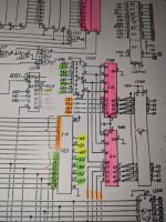
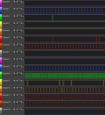
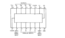
Decided to drill into the 083 implementation... There are four 74LS194 4-bit shift registers. They are clocked by the pixel clock (6MHz)... and they are loaded once every four pixels and then clocked out (in groups of 4 making up a colour)
JF_083_Shifter.png
Channels start at zero... so CH0 is pin 1 which is clock... Which should be a 6MHz pixel clock... and there it is!
pins 9 and 10 are used for load (when both are High) and then shifting when one is high... and hey presto there is it.. 4 pixels per load.
Nothing wrong there! (And looking at pins 12,13,14,15) on all of them they do seem to be shifting what they are getting.
 

NivagSwerdna

Active member
Feedback
1 (100%)
Credits
817CR
Got myself a little confused but have some spare time this evening...

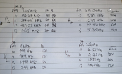
Small backtrack to document the video counters...
JFVideoCounters.png

Measure frequencies...
Channel numbers... to get pin numbers add 1...
JFVideoCountersNumbers.png
OK.. I'm confident those all look good... now time to go and measure the 74LS86s feeding the mux...
JFVideoXOR.png
On a real board I would know where things are but these are all over the place!
 

NivagSwerdna

Active member
Feedback
1 (100%)
Credits
817CR
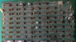
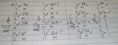
OK... so the game is to work out which XOR the A, B, C and D are equivalent to...
JFXORs.png
I can label the inputs because I happen to know what a Konami 082 does... and I know the frequencies so I can use this to identify which is which and if they are working...

JFXORMeasurements.png
So I know that A is equivalent to C13, B to D13, C to E12, D to E11. All of them look fine. (The HI comes from HFF; I won't argue). Two of the gates on D (equivalent to E11) are a bit random but I think they are unimplemented so it doesn't matter. So all good there... It's worrying that so much looks good... might have to try and attach a monitor again but first to map the MUXes... Looking for 4x 74LS153...

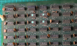
JFMuxPositions.png

Let's do this and then call it a night... 2hrs at a time is enough...
 

NivagSwerdna

Active member
Feedback
1 (100%)
Credits
817CR
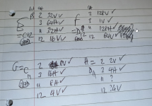
JFMuxes.png

So E is C12, F is D12, G is C11, H is D11. The inputs seem good and nothing obvious.

Might have to try adding my other monitor tomorrow... most of this seems feasible.
 

NivagSwerdna

Active member
Feedback
1 (100%)
Credits
817CR
Not making much progress... still cannot get monitor sync (I did actually swap out the 74LS244 as I suspected poor drive but didn't help) ... I decided I should avoid video for a bit and look at the 6809 side... however something else has broken now as I have no video counting at all... as I was tracing signals I noticed..

1729179329864.png

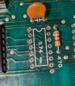
I'm quite intrigued by this.. I'm amazed I didn't spot it before... anyway... deserved to be whipped out to have a peak underneath...

1729179571862.png
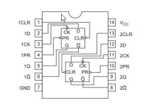
You can see that p5 and p9 are joined with a trace..


2024-10-17_17-28-58.png

p5 and p9 are obviously both outputs so this is a hardware bug.. the trace shouldn't go to pin 9. Cutting the pin works because 2Q isn't needed 2nQ is used.

Interesting.

Just got to get my clocks back now
 

NivagSwerdna

Active member
Feedback
1 (100%)
Credits
817CR
May as well keep the saga going... My de-soldering gun, SC-7000Z, is playing up... doesn't seem to be melting things the way it should and also seems to not suck as well as it did... On disassembly one of the ceramic bits at the back of the elements is snapped (looks like a pretty weak design) so need to replace that and also I'm not sure about the heating so that might be another job too...

Anyway...

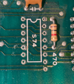
JF74Trace.png

This 74LS74 has annoyed me... so out with the 1977 vintage and in with a socket. I cut the trace to pin 9 under the new socket so no pins need to be cut anymore. The trace to the right goes nowhere in particular... I think that's right... if not I will apologise later.

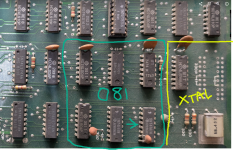
Still missing some fundamental signals... Looking at the board...

JF081.png
On a real JF there would be an 081 but here it is implemented in logic... It's quite like but not exactly the same as the attached schematic... the NANDS are replaced with ANDs and NORs and the gates are rearranged a bit differently (i.e. A and B parts in the 74LS74s swapped about a bit) but the gist is the same.

I suspect the second 74LS161 of having died in the interim... will whip that out if I can find some tinker time at the weekend.

PS

Quickly removed it..

1729287590193.png

About time something went my way... new one tomorrow...
 

Attachments

  • TK-707SUB_K81.pdf
    120 KB · Views: 6
Last edited:

NivagSwerdna

Active member
Feedback
1 (100%)
Credits
817CR
OK... a bit of time this Saturday evening...

Replaced the 161 which is the second part of the Konami 081 Counter Chain; lots of signals are back including sync (but my monitor arrangement still isn't convinced).

Whilst checking the signals I looked at the 74LS74 in the V counter chain (Konami 082) (circled green)...

JFPullup.png

and noticed...
JF74Glitch.png

The trouble is that once you've seen it... it is hard to un-see.

pins 4 and 10 shouldn't have glitches. They are active low pre-sets for the two parts of the 74LS74.

I will have to double check the traces but I think they are not being pulled hard enough and that one pull up resistor does quite a few pull-ups as it is shared the the pair of 161s; there is also an equivalent resistor in the H chain. I'm tempted to drop the value from 1k (marked on the board) to something smaller.

That being said the output signals do look OK.

(I did check voltages and they seem fine so not a droop effect).

Might fix that before moving on.

PS
So in the V counter chain the pull-up resistor does pins 4 and 10 on the 74LS74, pins 5 and 6 on the first LS161 and pins 3, 4, & 5 on the second LS161... i.e. pulls up 7 different pins. From memory you only need 10k for a single pin... so 1k should work for the combo. I'll see if I can find some 470 and replace both... sounds mostly harmless.
 
Last edited:

NivagSwerdna

Active member
Feedback
1 (100%)
Credits
817CR
OK... found some 690 Ohm resistors.. (was looking for 470 :) ) and...

JFGlitchGone.png

I must actually try and fix this thing at some point...

The glitches are gone; so that gives a nice warm fuzzy feeling.
 
Last edited:

NivagSwerdna

Active member
Feedback
1 (100%)
Credits
817CR
OK moving on to the main processor... 6809E... needs E and Q...

JFEandQ.png
Both E and Q are derived by the Konami 081 section but then make it up to a 74LS14 (hex schmitt inverter) up by the processor. The signals are buffered by the inverters... we should get E on pin 12 and Q on pin 8...

JFMeasuredEandQ.png

and we do... like magic.

Comparing to a 6809E timing diagram...

1729439188088.png
Looks nice. From the logic trace we see this is 1.5MHz i.e. 1/4 pixel rate and 1/12 of XTAL frequency.
The installed HD68A09E is capable of 1.5Mhz so all good there. (A MC6809E is 1MHz max)
18.432Mhz divided by 12 = 1.536MHz... close enough.

I won't touch on the slow CPU clock and what happens during a cycle at this point... I imagine we will get there later.
Suffice it to say that the DRAM addressing needs a faster clock to interleave the row and column addressing.

Next... look at RESET...
 

NivagSwerdna

Active member
Feedback
1 (100%)
Credits
817CR
RESET here we come...

JFnRESET.png
So the reset circuitry...

JFReset.png

So the principle of operation is that the 555 holds reset at power-up and then after that the nRESET is HI unless the counter H9 overflows... H9 is clocked by VBLANK and if it reaches 8 clocks with no intervening reset it causes a reset. The CPU has to reset it at least more frequently than 8 frames.

Anyway looking at I11

JF_I11.png
pins 8, 9, 10, 12, 13 are all High... not in reset... and it stays that way! That's a mighty good thing.
Look at WDT counter next...
 

NivagSwerdna

Active member
Feedback
1 (100%)
Credits
817CR
Looking at WDT Counter H9...

JFWDTCounterH9.png
A thing of beauty is a joy forever...
pin 10 (aka signal 216) is VBLANK... and it measures at 60.56Hz
pins 12&13 are the reset and we see it being reset every two frames
pin 5 is the LSbit of the counter... so it counts 0, 1 and then gets reset.

JFIntH12.png
So why two frames? Because H12 only generates an INT every two frames due to the H12 divide by two of signal 216
So the processor is running, not resetting, is interrupting, is watchdog counter resetting... A lot about this baby is humming!
 

NivagSwerdna

Active member
Feedback
1 (100%)
Credits
817CR
So now it's going to get geeky...

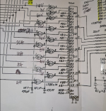
The equations of the decode PAL at B6 are..

Code:
Equations:

/o12 = i1 & i2 & /i3 & /i4 & i5
o12.oe = vcc

/o13 = i1 & i2 & i3 & i4
o13.oe = vcc

/o14 = i1 & i2 & i3 & /i4
o14.oe = vcc

/o15 = i1 & i2 & /i3 & i4
o15.oe = vcc

/o16 = i1 & i2 & /i3 & /i4 & /i5 & /i6 & /i7 & /i8 & /i9 & /i11
o16.oe = vcc

/o17 = i1 & i2 & /i3 & /i4 & /i5 & i6
o17.oe = vcc

/o18 = i1 & i2 & /i3 & /i4 & /i5 & /i6
o18.oe = vcc

/o19 = /i1 & /i4 & i6 & i7 & i9 & /o18
o19.oe = vcc

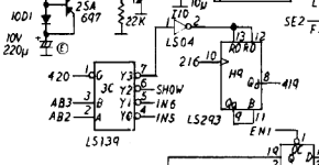
So we can work out what you need to address the WatchDog reset which is signal 420 and also AB2 = 1 and AB3 = 1 (decodes to 3 selects pin 7 active low)

1729457643039.png

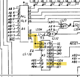
Now 420 is derived from the PAL...
1729457783676.png
And by the equations...
/o17 = i1 & i2 & /i3 & /i4 & /i5 & i6
Which requires AB15=1, AB14=0, AB13=0,AB12=0,AB11=1,AB10=X, AB9=X,AB8=X,AB7=X
and the the pin 14 output of A3 to be active also... AB6=0, AB5=0, AB4=1 and finally at 3C AB3=1 and AB2=1
So in bits... 1000 1XXX X001 11XX incompletely decoded... but something like $881C would fit.
But this doesn't agree with MAME...
Code:
    map(0x801c, 0x801c).r("watchdog", FUNC(watchdog_timer_device::reset_r));
which is curious.
Bleeped out the board and there is either an error on the schematic or the bootleg differs from the real thing...
The board is...
JFDecode.png

i.e. 17 and 16 are swapped on the schematic.
When we repeat the above using pin 16 we get...
/o16 = i1 & i2 & /i3 & /i4 & /i5 & /i6 & /i7 & /i8 & /i9 & /i11
i.e. 1000 0000 0001 11XX which gives $801C which matches MAME. Horray! It's incompletely decoded so access to 801C, 801D, 801E or 801F would work equally fine.
The swap also now puts the RAM at B7 at $8800-$8FFF which looks plausible.
Anyway that's my spare time for the w/e gone.. back to the grindstone.

PS
This makes INTST 1000 000 0011 X000 i.e. $8030 (or $8038)
Code:
map(0x8030, 0x8037).w("mainlatch", FUNC(ls259_device::write_d0));
...
mainlatch.q_out_cb<0>().set(FUNC(junofrst_state::irq_enable_w));
I should have enough info to use the Retro Processor Electron Wrangler...
 
Last edited:

NivagSwerdna

Active member
Feedback
1 (100%)
Credits
817CR
I'm still after some video output... de-soldered the 74LS240 on the video outputs (the video DAC), tested OK, put in a socket... no change.
This doesn't really make much sense... just getting blackness out...
Decided to look at the Colour Palette RAMs
1729631664342.png
These are written to when 118 is LO (pin is really nWE)
I would hope these would be random on power-up giving some output but I am just getting black... I really don't like the theory that these are an issue as they have inverting data outputs so would actually give White not black for zero; also one might fail but both? Seriously clutching at straws here..
Anyway let's see when they are written.
JF_A3_SE1.png
This is A3... Channels are numbered from 0 so p15 which is SE1 is found at CH14. You can see it is intermittently active (active LOW); so we have writes to the palette RAM. (TBH the main CPU seems to be running nicely).
There seem to be sets of eight double dips every 30Hz... i.e. every two frames (and we know the video interrupt is every two frames).
This might suggest we write the entire 16 bytes (4 bits x 16 in each 7489 every video interrupt)...
Looking at MAME...
JFPalletteWrites.png
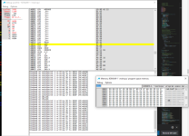
Every two VBLANKS it writes to the whole Colour Palette... The early colours remain the same (for a few double frames at least) and some of the higher colours are changing, probably to give a video effect.
So all that stuff seems to be working... might have to have a think... if not... I guess I need to stare at the 7489s...
 

NivagSwerdna

Active member
Feedback
1 (100%)
Credits
817CR
So here we are again... another night on the PCB... I'm hunting pixels...

Everything looks good at the Palette RAM so moving into the Konami 083 section...

JFK83Section.png

There's something not right...

1729719248834.png

I don't know if I am going mad... but pin 1 (CH0) should not be LOW.

1729719335360.png
Pin 1 is clear... active LOW... and it appears LOW! But the outputs are not all low.
I think Pin 1 should be HI... Looked at the PCB seems all Pin 1s of the 74LS194s are not connected to anything!
Am I going mad?
Decided to remove them anyway to see if there was a trace I couldn't see...
1729719549652.png
Wot no pin 1 connections on top?
1729719620459.png
Wot no pin 1 connections on the bottom!
The devices themselves are all good; which is what I expected. Will put them back with some kind of bodge to pull pin 1s HI
@Alpha1 just curious did this board ever work? Maybe the inputs should float high so this is a red Herring. This is very fun though.
 
Last edited:

cliff_poole

Active member
vacBacker
Feedback
6 (100%)
Credits
1,069CR
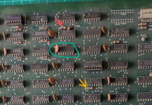
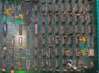
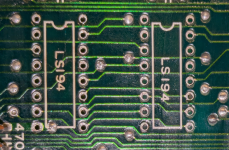
I dug out my board. All the 74LS194s in that position on mine also have pin 1 left floating.

Mine also has the snipped chip leg.

Juno1.jpg

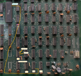
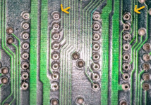
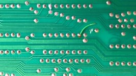
Does yours also have the following cut track on pin 15 of the 74LS367 in the position below ?. Ignore the bit of kynar wire, that was where I patched it at first before working out that it was probably a factory mod.

Juno2.jpg
Juno3.jpg
 
Top