Another recent pick up from alpha1 who reported the following issues .... green only screen, graphics issues, some sounds present ... here are his pics ...

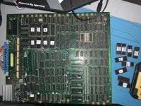
Board arrived in decent shape, nothing obviously missing, just a bit dusty/grimy as expected ..... Interesting board .... I have another Wonder Boy bootleg with just one (large) daughter board but this one has a (medium) daughter board to replace the 3x sega 5025 chips under ROM's 6/7/8 but that is quite normal - seems to be quite common to have this. The other (small) daughter board though (the one near the jamma edge connector) I think is less common and contains a Z80, PROM and a couple of TTL chips...

Before plugging in I gave it a clean, and dumped the ROMs. A mish mash of various rom sets with some coming from the US bootleg set (sprites) , some from the 4D Warriors conversion set (tiles) and one (ROM 3) from Set3. Two ROMS I couldn't identify at all - The other main cpu rom - ROM 1 (I'm guessing because it had no sticker), and the sound ROM also didn't identify but when verified with the common Wonder Boy sound rom it showed just the odd byte different.
Gave the usual visual once over, looking for any obvious signs of problems before powering up. Found a couple of pins on the medium sized daughter board touching and a few areas on the solder side of the pcb where it looked like pins could be touching and traces had been scratched or potentially broken, shown on the pic below .....

Straightened out any touching pins I could see and checked for shorts (all good) and powered up for the first time ....

Good to see all colours present and correct, but clearly not all is well ... Game seems to be running fine, just some messed up graphics. Looks like it's mainly confined to the text/character layer on the game play screen, but on the high score screen there is a patch in the middle of the screen where text is fine ...
Went looking specifically for the text/character ROM but it seems that's just contained in the 'tiles' roms (6, 7, 8) Probing address and data pins showed good activity. Nothing missing anyway. Some signals did seem to be a bit 'noisy' but no big red flags. The RAM under the big daughter board was similar, had really clean looking address signals but data lines again a little noisy .... At that point though I was looking for floating or stuck signals and didn't find any ...
At this point I flipped the pcb and gave it a proper check, all those areas where I thought there may be damaged traces and checked those and looked for other signs of issues. All the traces were OK though and no loss of continuity anywhere ....
Went back to the tiles ROMs and had more of a poke around looking at those signals that just didn't look right. Found a LS273's @ V10 connected to the ROM address lines which also carried these odd looking signals... the clock signal on pin 11 looked the same,, which I thought odd, especially when compared with the signal on the LS273 @ W10 right above it. Much cleaner ... The suspect clock signal (left) on V10 compared to the cleaner clock signal (right) on W10 ....

Didn't like the look of it so SLICED the 273 and as you can see it failed pretty badly ... that was enough to convince me it was bad and so out it came ...

Popped in a replacement LS273 and fired her up, convinced I'd found the suspect and would see at least some improvement, if not the graphics fully restored .....
But no ... no difference made at all. Replacement chip was also failing slice and all signals were the same as before ...
Must be something connected to the 273 then making if fail .. had to be ... I'd traced the clock signal earlier with continuity to a LS174 under the medium daughter board, but didn't really think too much about it then. Now I checked the source if the clock on the other (non dodgy) 273 and it was connected to a LS163 over on the other side of the board. And then I re-checked the dodgy 273's clock and it was also connected to the LS163... But the non dodgy 273 wasn't connected to the LS174 .... And then it clicked there must be a bridge somewhere ... Didn't take too long to find it once I knew which traces to follow ...

And when I see it there on that picture I wonder how the hell I didn't see it when I gave it a 'proper' check over earlier !!
So I break the bridge and of course this cleans up all the graphics issues completely .....

Wonder Boy in all it's visual glory !!
Just the sound issue remains... all sound effects were working great, just no music at all ..... tbc
Board arrived in decent shape, nothing obviously missing, just a bit dusty/grimy as expected ..... Interesting board .... I have another Wonder Boy bootleg with just one (large) daughter board but this one has a (medium) daughter board to replace the 3x sega 5025 chips under ROM's 6/7/8 but that is quite normal - seems to be quite common to have this. The other (small) daughter board though (the one near the jamma edge connector) I think is less common and contains a Z80, PROM and a couple of TTL chips...
Before plugging in I gave it a clean, and dumped the ROMs. A mish mash of various rom sets with some coming from the US bootleg set (sprites) , some from the 4D Warriors conversion set (tiles) and one (ROM 3) from Set3. Two ROMS I couldn't identify at all - The other main cpu rom - ROM 1 (I'm guessing because it had no sticker), and the sound ROM also didn't identify but when verified with the common Wonder Boy sound rom it showed just the odd byte different.
Gave the usual visual once over, looking for any obvious signs of problems before powering up. Found a couple of pins on the medium sized daughter board touching and a few areas on the solder side of the pcb where it looked like pins could be touching and traces had been scratched or potentially broken, shown on the pic below .....
Straightened out any touching pins I could see and checked for shorts (all good) and powered up for the first time ....
Good to see all colours present and correct, but clearly not all is well ... Game seems to be running fine, just some messed up graphics. Looks like it's mainly confined to the text/character layer on the game play screen, but on the high score screen there is a patch in the middle of the screen where text is fine ...
Went looking specifically for the text/character ROM but it seems that's just contained in the 'tiles' roms (6, 7, 8) Probing address and data pins showed good activity. Nothing missing anyway. Some signals did seem to be a bit 'noisy' but no big red flags. The RAM under the big daughter board was similar, had really clean looking address signals but data lines again a little noisy .... At that point though I was looking for floating or stuck signals and didn't find any ...
At this point I flipped the pcb and gave it a proper check, all those areas where I thought there may be damaged traces and checked those and looked for other signs of issues. All the traces were OK though and no loss of continuity anywhere ....
Went back to the tiles ROMs and had more of a poke around looking at those signals that just didn't look right. Found a LS273's @ V10 connected to the ROM address lines which also carried these odd looking signals... the clock signal on pin 11 looked the same,, which I thought odd, especially when compared with the signal on the LS273 @ W10 right above it. Much cleaner ... The suspect clock signal (left) on V10 compared to the cleaner clock signal (right) on W10 ....
Didn't like the look of it so SLICED the 273 and as you can see it failed pretty badly ... that was enough to convince me it was bad and so out it came ...
Popped in a replacement LS273 and fired her up, convinced I'd found the suspect and would see at least some improvement, if not the graphics fully restored .....
But no ... no difference made at all.
Replacement chip was also failing slice and all signals were the same as before ...Must be something connected to the 273 then making if fail .. had to be ... I'd traced the clock signal earlier with continuity to a LS174 under the medium daughter board, but didn't really think too much about it then. Now I checked the source if the clock on the other (non dodgy) 273 and it was connected to a LS163 over on the other side of the board. And then I re-checked the dodgy 273's clock and it was also connected to the LS163... But the non dodgy 273 wasn't connected to the LS174 .... And then it clicked there must be a bridge somewhere ... Didn't take too long to find it once I knew which traces to follow ...
And when I see it there on that picture I wonder how the hell I didn't see it when I gave it a 'proper' check over earlier !!
So I break the bridge and of course this cleans up all the graphics issues completely .....
Wonder Boy in all it's visual glory !!
Just the sound issue remains... all sound effects were working great, just no music at all ..... tbc
Last edited: