Fixing an Alcon/Slap Fight PCB

myPinballs

Active member
Feedback
16 (100%)
Credits
668CR
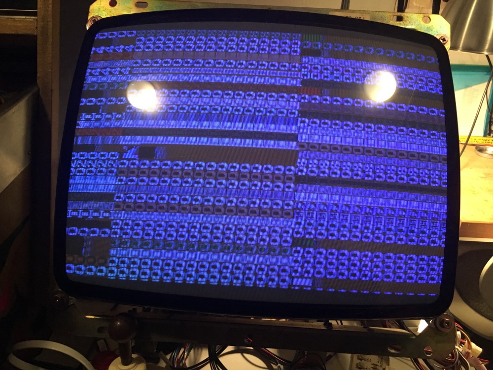
From my board repair i'm still stuck on this screen

IMG_0698.jpg


Though i have worked out that i can change some of the characters on screen by shorting various lines of the data buffers for the foreground and background ram. So i need to think more as to why its not all zeros.

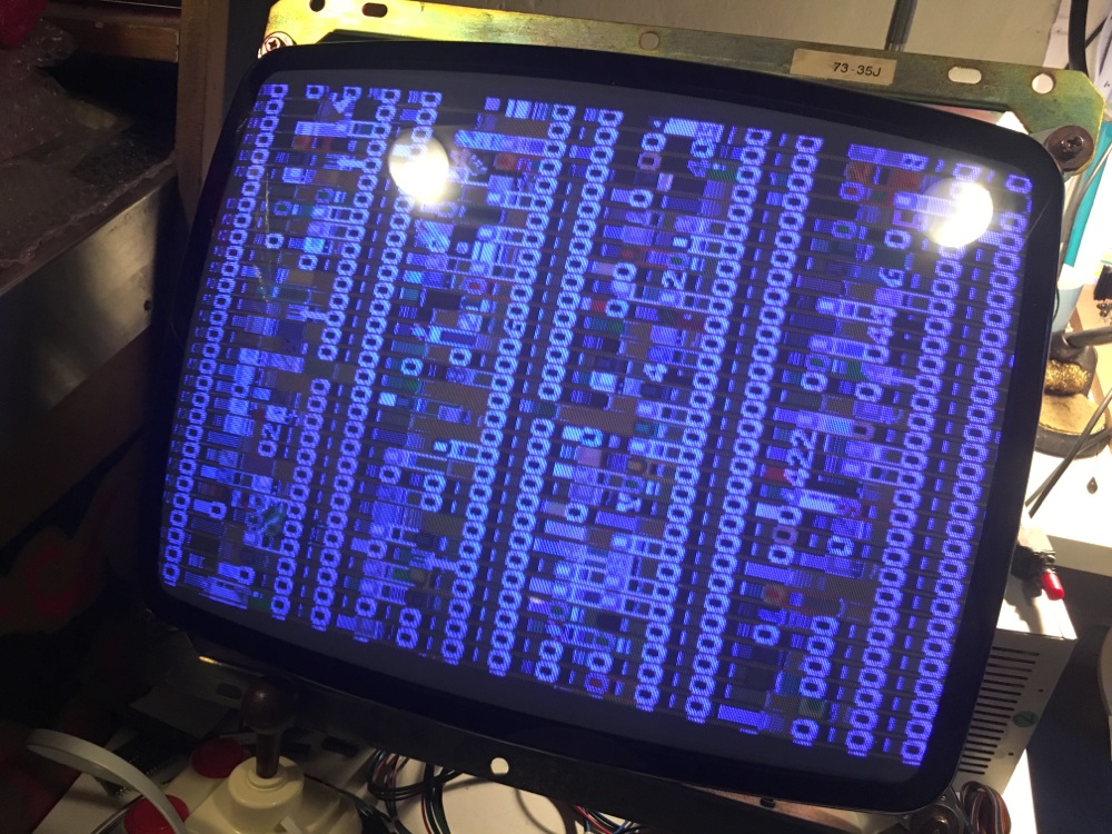
Also, i don't get a solid picture all the time still, sometimes its not synced and it just lines or noise. I think i may have worked out the likely culprit here as can tell what isn't pulsing when the image disappears.

Traced it to the horizontal section chips 1F & 2F and 1D which i think one or more are failing. They are the starting point for the vertical section line clock. They are 74LS669 ics so ordering some to replace and try out shortly.

Fingers crossed.

myPinballs2018-01-17 12:26:06
 

John Bennett

Senior Member
vacBacker
Feedback
10 (100%)
Credits
4,979CR
Is the screen full of zeroes the 'leftovers' after it does a RAM test on the foreground RAM? (so it's just whatever is left in that RAM after a test, which happens to correspond to a screen of '0's)

If so, I'd have thought the processor would have a relatively large time window to populate that RAM (i.e. many milliseconds) before the video hardware buffers it. Or it might've done it leisurely over many screen refreshes as it's not intended to look nice.
If so, it could've been happily testing that RAM, inbetween doing other tasks, but it then crashed. If so, what's on the screen might not help you much in debugging - just shows it didn't finish what it was doing.
Are the main CPU RAM and it's interconnections OK? (assuming it's not fixed after sorting the counter circuit).John Bennett2018-01-17 18:56:42
 

Judder

Active member
Feedback
2 (100%)
Credits
992CR
Judder repair:

(BTW tell me if easier to put this in a separate thread and totally happy to do so!)

So on myPinballs advice I focused on the top (with connector) board that does the Audio and some of the sprites as this seems to be crashing the CPU boot process

From probing the Chip Enable pin of AR_02 - the audio EPROM - I can see that on power on it goes high, but then drops to no power after a number of seconds / milli-seconds

My thoughts are that this is probably due to a capacitor being dead and grounding to 0 as the longer the PCB has no power, the slower it takes to reduce to no signal

Any thoughts on where to look?!

Here's a video of it doing exactly that (pin 20 of the 2764 CE)


Mitchell Gant

Active member
vacBacker
Feedback
2 (100%)
Credits
884CR
John Bennett said:
Is the screen full of zeroes the 'leftovers' after it does a RAM test on the foreground RAM? (so it's just whatever is left in that RAM after a test, which happens to correspond to a screen of '0's)

If so, I'd have thought the processor would have a relatively large time window to populate that RAM (i.e. many milliseconds) before the video hardware buffers it. Or it might've done it leisurely over many screen refreshes as it's not intended to look nice.
If so, it could've been happily testing that RAM, inbetween doing other tasks, but it then crashed. If so, what's on the screen might not help you much in debugging - just shows it didn't finish what it was doing.
Are the main CPU RAM and it's interconnections OK? (assuming it's not fixed after sorting the counter circuit).

I stepped through the first part of the code in MAME debugger a couple of days ago, which I'd done before a few years ago. After reset it sets/clears some I/O ports for interrupts, ROM bank, screen flip and audio interrupts using the LS259 latch at 9J, then enters the RAM test loop. MAin CPU interrupts are DISABLED during RAM test.

The RAM test is pretty crude, it writes $FF to each location then subtracts what it reads back from that location, tests that it's zero, stores that and again subtracts what it reads back and tests for zero again.

It starts with an 8K block starting at $C000. This is all the background RAM. Then it does a 4K block at $F000 which is character/colour RAM which you will see on screen. This leaves all zeroes (that also by coincidence show as character '0' on screen) in the RAM.

So if you're seeing a full screen of '0's it shows the main CPU has run at least some code OK, at least for a few milliseconds as you say to fill the 10K or so of RAM during test.

Stepping further into the code after that shows that it then blanks out the character RAM to $2D, which is a blank character, and prints the result of the RAM test.

So it seems like it's failing at some point after doing the RAM test, but before the block fill of blanks characters to the screen. I'm not sure at this point what could cause such a failure without a bit more MAME debugging. I'll try and keep digging.
 

Mitchell Gant

Active member
vacBacker
Feedback
2 (100%)
Credits
884CR
Judder said:
Judder repair:

From probing the Chip Enable pin of AR_02 - the audio EPROM - I can see that on power on it goes high, but then drops to no power after a number of seconds / milli-seconds

My thoughts are that this is probably due to a capacitor being dead and grounding to 0 as the longer the PCB has no power, the slower it takes to reduce to no signal

Any thoughts on where to look?!

Not sure what I'm seeing here but it looks like your 5V power is failing? What does your 5V line read, say across that EPROM you're probing there. (i.e. between pins 14 and 28)
 

Judder

Active member
Feedback
2 (100%)
Credits
992CR
Mitchell Gant said:
Not sure what I'm seeing here but it looks like your 5V power is failing? What does your 5V line read, say across that EPROM you're probing there. (i.e. between pins 14 and 28)

Thanks for the reply MG

14 - 28 stays constant +5V at all times

14 - 20 (_CE_) starts off at 4.9V and then just slowly drops over time to 3.8, 3.7 etc

My thoughts would be that Chip Enable being negative activated should go to 0 straight away

Problem with the 2nd Z80 controlling that side of the board?

That particular EPROM verified fine, so I'm wondering if something else broken or shorting is giving drain on the board but not effecting the +5V and GND circuit mains

The slow drain feels like capacitors but that's just a thought...

Indeed a challenging one!
 

myPinballs

Active member
Feedback
16 (100%)
Credits
668CR
John Bennett said:
Is the screen full of zeroes the 'leftovers' after it does a RAM test on the foreground RAM? (so it's just whatever is left in that RAM after a test, which happens to correspond to a screen of '0's)

If so, I'd have thought the processor would have a relatively large time window to populate that RAM (i.e. many milliseconds) before the video hardware buffers it. Or it might've done it leisurely over many screen refreshes as it's not intended to look nice.
If so, it could've been happily testing that RAM, inbetween doing other tasks, but it then crashed. If so, what's on the screen might not help you much in debugging - just shows it didn't finish what it was doing.
Are the main CPU RAM and it's interconnections OK? (assuming it's not fixed after sorting the counter circuit).

Mitchell Gant said:
I stepped through the first part of the code in MAME debugger a couple of days ago, which I'd done before a few years ago. After reset it sets/clears some I/O ports for interrupts, ROM bank, screen flip and audio interrupts using the LS259 latch at 9J, then enters the RAM test loop. MAin CPU interrupts are DISABLED during RAM test.

The RAM test is pretty crude, it writes $FF to each location then subtracts what it reads back from that location, tests that it's zero, stores that and again subtracts what it reads back and tests for zero again.

It starts with an 8K block starting at $C000. This is all the background RAM. Then it does a 4K block at $F000 which is character/colour RAM which you will see on screen. This leaves all zeroes (that also by coincidence show as character '0' on screen) in the RAM.

So if you're seeing a full screen of '0's it shows the main CPU has run at least some code OK, at least for a few milliseconds as you say to fill the 10K or so of RAM during test.

Stepping further into the code after that shows that it then blanks out the character RAM to $2D, which is a blank character, and prints the result of the RAM test.

So it seems like it's failing at some point after doing the RAM test, but before the block fill of blanks characters to the screen. I'm not sure at this point what could cause such a failure without a bit more MAME debugging. I'll try and keep digging.

Thank you both very much for the replies above. The tech info from Mitchell is particularly useful and much appreciated.

I did change and socket the main cpu 'scratch' ram ic before when originally looking at this but it didnt make any difference. Good to rule it out though.

IMG_0714.jpg


Very interesting notes on the ram test. So the ram test is only the background and foreground rams that are being tested? Makes sense that the sound ram would be part of the later sound test, but what about the sprite ram? And yes from what you say it does look like my board set has 2 issues with the ram section:

1) Something is up when its writing and or reading back the test FF data as it shows different characters at some positions. So i assume this is foreground/char data from other locations instead of the expected 0.

2) When it gets to the blank screen instruction call the cpu crashes, or just before this.

What i'm thinking at the moment is a possible data line buffer fault perhaps, beacuse these chips are all tied to the main cpu data bus. I've seen this many times before where 1 chip with a stuck line can cause an issue what sends the cpu off into the weeds! The problem i've come across to though is sometimes the buffers look to be functioning ok from a logic probe test.

Really looking forward to seeing what else you can find in the mame code.

Currently waiting for these 74LS669 ics to arrive so i can hopefully resolve the screen issue and get on with the rest of the fix.
 

myPinballs

Active member
Feedback
16 (100%)
Credits
668CR
IMG_0698.jpg


1 final thought on my ram screen. I may be trying to see things that aren't there, but there is a kind of pattern to it, where some of the vertical lines are correct. Could this be tied to the data lines or not??? Hmmmm

Taking a count of character blocks from left to right and working in block of 8. It seems like the vertical columns with the '0' character in relate to a repeat of 1 and 7 if you count 0,1,2,3,4,5,6,7 and then repeat.

myPinballs2018-01-18 09:44:11
 

Mitchell Gant

Active member
vacBacker
Feedback
2 (100%)
Credits
884CR
myPinballs said:
1 final thought on my ram screen. I may be trying to see things that aren't there, but there is a kind of pattern to it, where some of the vertical lines are correct. Could this be tied to the data lines or not??? Hmmmm

Taking a count of character blocks from left to right and working in block of 8. It seems like the vertical columns with the '0' character in relate to a repeat of 1 and 7 if you count 0,1,2,3,4,5,6,7 and then repeat.

Yeah I was trying to see a pattern in your photo too!

Your monitor is rotated anti clockwise as Slap Fight is a vertical game. In your photo the lowest address would be the lower right corner, on a proper game cab this would be bottom ** left **. Incrementing addresses then work their way UP the game screen (to the left on your photo), then wrap back to next column. Hope that makes some sense...

One question I have for you is to ask if that image you took in the photo is ALWAYS the same pattern after several power cycles hours or days apart? If so then it shows that the CPU is actually writing the same zeros. If not then it may well be simply the RAM contents have some pattern of zeroes when you took that photo. I realise the junk characters may well change, but are the zeros always in the same position?
 

myPinballs

Active member
Feedback
16 (100%)
Credits
668CR
Mitchell Gant said:
Yeah I was trying to see a pattern in your photo too!

Your monitor is rotated anti clockwise as Slap Fight is a vertical game. In your photo the lowest address would be the lower right corner, on a proper game cab this would be bottom ** left **. Incrementing addresses then work their way UP the game screen (to the left on your photo), then wrap back to next column. Hope that makes some sense...

One question I have for you is to ask if that image you took in the photo is ALWAYS the same pattern after several power cycles hours or days apart? If so then it shows that the CPU is actually writing the same zeros. If not then it may well be simply the RAM contents have some pattern of zeroes when you took that photo. I realise the junk characters may well change, but are the zeros always in the same position?

Hi yes i understand what you are saying and therefore the bits showing the zero lines would be 1 & 3 if we take the first column as 0 which is half off the screen on the right of my picture.

I think the image is always the same (in terms of zeros)

Here is a pic taken a few months earlier, when i was first looking at the issue (31st august 2017)

IMG_9719.jpg


Maybe what we are seeing is some sort of addressing issue, where the cpu is only able to write successfully to a certain portions of ram and the other stuff is just what gets converted as characters from the garbage left in the ram at power on??

Does seeing some zeros indicate the data line buffers are working correctly?

myPinballs2018-01-18 13:27:02
 

myPinballs

Active member
Feedback
16 (100%)
Credits
668CR
Worked out a few other things today with my board. Found that there is a sprite ram section on the main cpu board at 2L. If you short some of the data lines on the buffer chip to this ram then you can change the screen pattern as above.

I also found a small mistake on the schematics. (Hope you ok with feedback on them Mitchell, happy to report things as i find them)

The inputs for 2k:D and 2k:C on page 9 are labelled wrong

2K:D pin 12 is !SPRITE_RAM

2K:D pin 13 is !WR

2K:C pin 9 is !MREQ

2K:C pin10 is !SPRITE_RAM

At first i thought i had found a bad trace as the MREQ line wasn't linking over, but then i found the error in the schematics.

The !SPRITE_RAM enable though just stays high on the board, which is created from 9K. One this chip all other enable lines (except !MCU_PORT) inc the background ram ones seem to pulse so that makes sense with what we talked about earlier to.

Only the rom at 8P is enabled. I guess this is because the boot code if accessed from there only so 8N is not used till later
 

Mitchell Gant

Active member
vacBacker
Feedback
2 (100%)
Credits
884CR
myPinballs said:
Worked out a few other things today with my board. Found that there is a sprite ram section on the main cpu board at 2L. If you short some of the data lines on the buffer chip to this ram then you can change the screen pattern as above.

I also found a small mistake on the schematics. (Hope you ok with feedback on them Mitchell, happy to report things as i find them)

Yeah absolutely I welcome feedback for mistakes! I spent a lot of days over Christmas 2014 with a multimeter and a Tiger Heli board to trace this schematic out. There are bound to be many mistakes, even though I spotted a few during tracing. I didn't spend so much time tracing the Slap Fight board apart from the RAM access WAIT logic which is the major difference between that and Tiger Heli.

Tiger Heli can only access background and foreground RAM when it uses a Z80 output port instruction to turn off graphics access to those RAMs. This can only be done during vertical refresh or the screen would blank and flicker.

With Slap Fight they added the extra logic to force the Z80 into a wait state to let the screen logic keep the picture output but also allow software access any time rather than just vertical refresh period.

myPinballs said:
The inputs for 2k:D and 2k:C on page 9 are labelled wrong

2K:D pin 12 is !SPRITE_RAM

2K:D pin 13 is !WR

2K:C pin 9 is !MREQ

2K:C pin10 is !SPRITE_RAM

At first i thought i had found a bad trace as the MREQ line wasn't linking over, but then i found the error in the schematics.

I'll label the schematics with your text above, but do do the actual changes 'til I've had time to compare the Tiger Heli board I originally traced. It may be that there are minor differences between the boards as well as the WAIT logic and the 2x 74LS194's instead of a 74LS299 for the pixel shift registers.

myPinballs said:
The !SPRITE_RAM enable though just stays high on the board, which is created from 9K. One this chip all other enable lines (except !MCU_PORT) inc the background ram ones seem to pulse so that makes sense with what we talked about earlier to.

Only the rom at 8P is enabled. I guess this is because the boot code if accessed from there only so 8N is not used till later

If it stops in a loop part way through start up test like we think it will not select the upper ROM area and banked ROM area that is the 8N chip, so you won't see it enabled. Same goes for the sprite RAM enable.

From a quick look and a guess with your zeroes "pattern" I'd be checking the '157 multiplexer at 3H (does A0 to A3 so maybe the every 8 line pattern?)
 

myPinballs

Active member
Feedback
16 (100%)
Credits
668CR
Mitchell Gant said:
From a quick look and a guess with your zeroes "pattern" I'd be checking the '157 multiplexer at 3H (does A0 to A3 so maybe the every 8 line pattern?)

Yes, exactly what i was thinking to. I did test 3H, 3G & 3F though and all seemed to pulse ok, though i'm not sure if you can always tell. I'm going to change 3H tomorrow anyway just to see what changes!
 

myPinballs

Active member
Feedback
16 (100%)
Credits
668CR
Well, i changed ic 3H and no different. I then changed ic 2D which is before the chips 3H, 3G, 3F and something odd happened. At the first power up i got a message saying RAM CHECK OK, but was repeated 16 times down the screen, then the next power up i got a RAM CHECK ERROR message with a similar number of repeats, and then the 3rd power up back to the zeros screen but now its different. I have been poking around with the logic probe for hours and hours today trying to see what i can find out but still stuck here. I didn't get a picture of the ram check screen either which is annoying me.

IMG_0721.jpg
IMG_0722.jpg


myPinballs2018-01-19 19:14:50
 

Mitchell Gant

Active member
vacBacker
Feedback
2 (100%)
Credits
884CR
Yeah that's annoying that you saw RAM CHECK OK for a brief time then no more. Something has definitely changed though from the photo.

Latch at 2D (I assume a 74LS374) is part of the video output section and in itself cannot cause the RAM test to fail, only affect video output. You could in theory remove that chip and the game would play blind but otherwise pass test and run normally. So it looks like there are multiple faults on your board I'm afraid.

Do you have an EPROM programmer and eraser? Maybe it's time to start writing some test code and see what results show on screen then. I did write a little bit for Tiger Heli/Slap Fight so if I can find that maybe we could narrow it down better than the crude default game test. Something like writing 0123456789ABCDEF and repeating rather than all 0's.
 

myPinballs

Active member
Feedback
16 (100%)
Credits
668CR
Yeah I think the 74ls374 at 2D helped abit with the picture stability.

Certainly have an eprom burner and eraser as use them daily. I burned new roms as a first step when starting to look at the board. If you have some test roms then that would be great. Anything that can help narrow my diagnostic search would be greatly received !
 

Judder

Active member
Feedback
2 (100%)
Credits
992CR
Quick update:

I removed all of EPROMs from the top Audio CPU board to see if they were being used during boot and Mitchell is correct that only EPROMs A0 and A1 on the lower board Main CPU are used - you need both of these in place for the self check to run (tested by removing one and the self test failing)

Removing and/or swapping the colour PROMs @ Rom 19, 20 and 21 I can change the colours of the screen output, and get character output from the self test by disconnecting the audio board from the main board, so the video part is definitely running

So... I'm thinking that my issue is around RAM as it hangs at this point in the self test

Mitchell Gant said:
The RAM test is pretty crude, it writes $FF to each location then subtracts what it reads back from that location, tests that it's zero, stores that and again subtracts what it reads back and tests for zero again.

It starts with an 8K block starting at $C000. This is all the background RAM. Then it does a 4K block at $F000 which is character/colour RAM which you will see on screen. This leaves all zeroes (that also by coincidence show as character '0' on screen) in the RAM.

So if you're seeing a full screen of '0's it shows the main CPU has run at least some code OK, at least for a few milliseconds as you say to fill the 10K or so of RAM during test.

@Mitchell - From the above RAM test could you point out which RAM chips are used as the background RAM and which as the character/colour RAM please?

The reason to ask is that the 4 x 2148 chips on the top Audio CPU board get incredibly hot during my tests so I'm wondering if socketing and / or replacing those might be my next best step?
 

Mitchell Gant

Active member
vacBacker
Feedback
2 (100%)
Credits
884CR
Judder said:
Quick update:

@Mitchell - From the above RAM test could you point out which RAM chips are used as the background RAM and which as the character/colour RAM please?

The reason to ask is that the 4 x 2148 chips on the top Audio CPU board get incredibly hot during my tests so I'm wondering if socketing and / or replacing those might be my next best step?

On the CPU board (one without edge connector) chips 4c and 4F are the foreground character/colour RAMs.

Also on CPU board chips at 4N and 4P are background RAM.

I think socketing RAMs like this is always a good idea, as long as you are confident you can do it without damaging the PCB and causing more faults.

The 4x 2148's are sprite line buffer RAM, and it's normal for them to run pretty hot, too hot to touch sometimes. If they are faulty, they would not be able to stop the startup test from running (they're not accessible from the CPU).

Do you have access to an EPROM programmer and UV eraser? If so I'm working my way to making a test EPROM that could give a better idea of faults than the built in game test. myPinballs has been helping me test the test
smiley20.gif
 

myPinballs

Active member
Feedback
16 (100%)
Credits
668CR
Judder said:
Quick update:

I removed all of EPROMs from the top Audio CPU board to see if they were being used during boot and Mitchell is correct that only EPROMs A0 and A1 on the lower board Main CPU are used - you need both of these in place for the self check to run (tested by removing one and the self test failing)

Removing and/or swapping the colour PROMs @ Rom 19, 20 and 21 I can change the colours of the screen output, and get character output from the self test by disconnecting the audio board from the main board, so the video part is definitely running

So... I'm thinking that my issue is around RAM as it hangs at this point in the self test

@Mitchell - From the above RAM test could you point out which RAM chips are used as the background RAM and which as the character/colour RAM please?

The reason to ask is that the 4 x 2148 chips on the top Audio CPU board get incredibly hot during my tests so I'm wondering if socketing and / or replacing those might be my next best step?

It would be easier to quote ram and chip as per the board position if possible :) , as this is what the schematics use and how i and Mitchell have been identifying things. The rom names from mame are weird!

Foreground RAM (Character) is 4F

Foreground Ram (Attributes) is 4G

myPinballs2018-01-22 13:21:40
 
Top