NivagSwerdna
Active member
To conclude the Sprite Generation hardware I need to consider graphic bank switching...
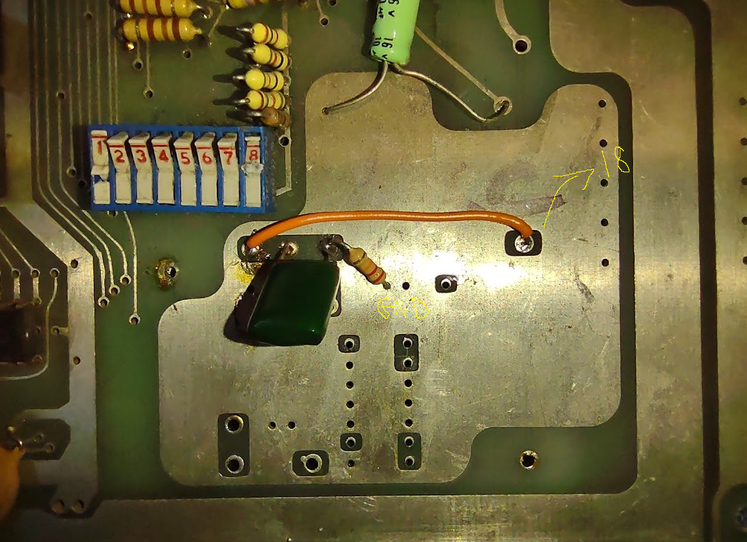
Galaxian does not switch banks, however Moon Cresta requires extra addressing to cover the larger (2532 Graphics ROMs); to facilitate this the driver latch at 6000 is re-purposed from 1P Start LED, 2P Start LED and Coin Lockout to 3 bits of bank switching data. The driver latch 9M is also moved from 6000 to A000 in the memory map.
The upshot of this is that you effectively get 3 1-bit registers at A000, A001 and A002.
A002 is effectively "Bank Switch Enable", and A001 and A000 are bank number.
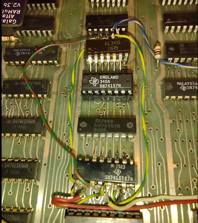
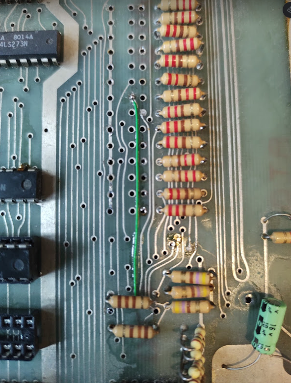
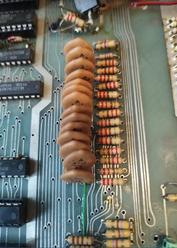
To accomplish this the bodge is as follows... An extra 74LS157 mux is mounted on 3J and a 74LS10 triple input NAND on top of 3M.
The extra inputs from 9M are routed via wires that cross the board.
The upshot of this is when A002 is 0 the original Galaxian scheme is followed but when A002 is 1 then A9 is driven by latch A000 and A10 is driven by latch A001. (Actually not all of the address space... the triple input NAND is used to stop some sprite remapping)
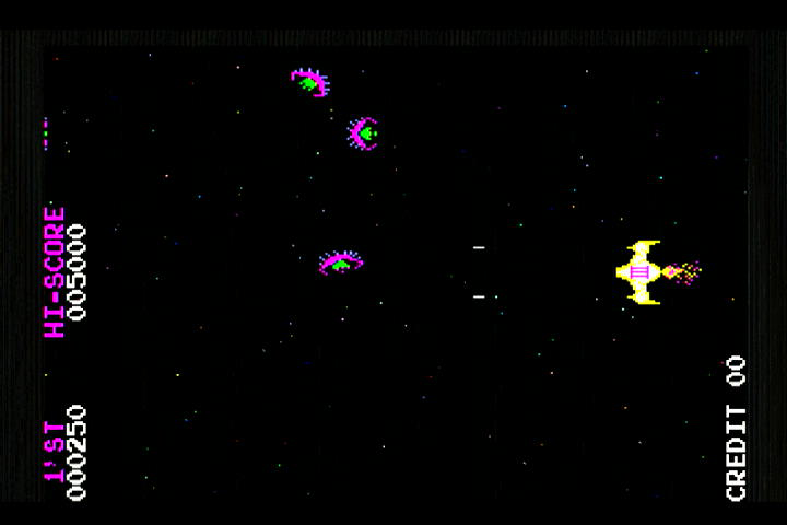
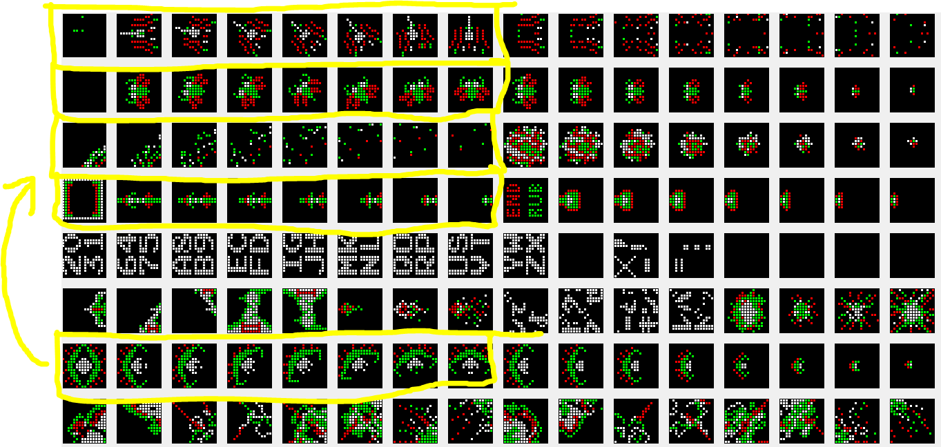
Anyway... we can see the effect by setting up some Sprites...
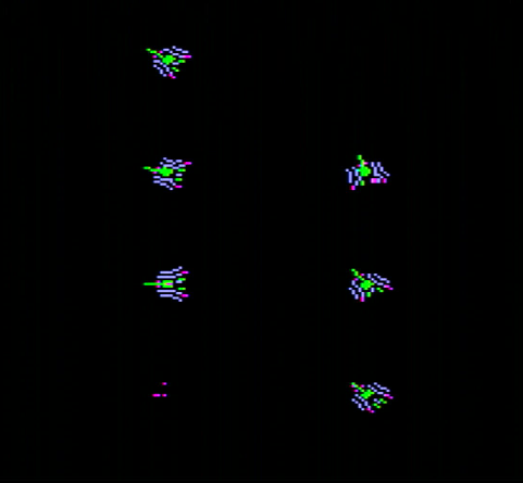
With A000..2 set to 000... i.e. no remap
Sprites 20, 21, 22, 23, 24, 25, 26 (hex)...
then changing the banking...
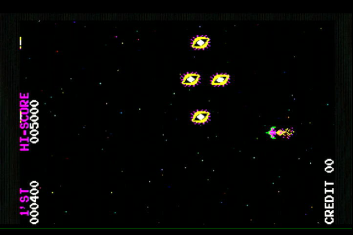
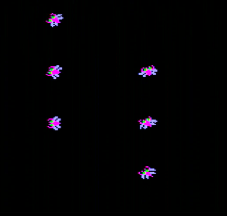
With A000..2 set to 100... i.e. remap, bank 00
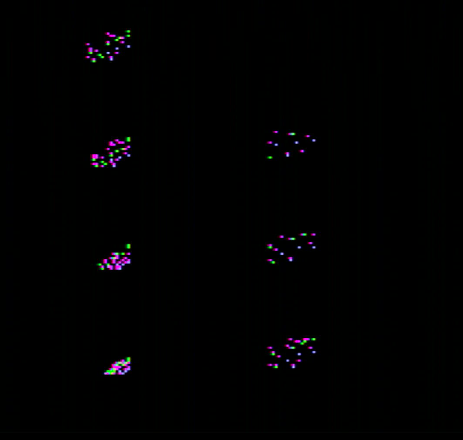
With A000..2 set to 101... i.e. remap, bank 01
With A000..2 set to 110... i.e. remap, bank 10
With A000..2 set to 111... i.e. remap, bank 11
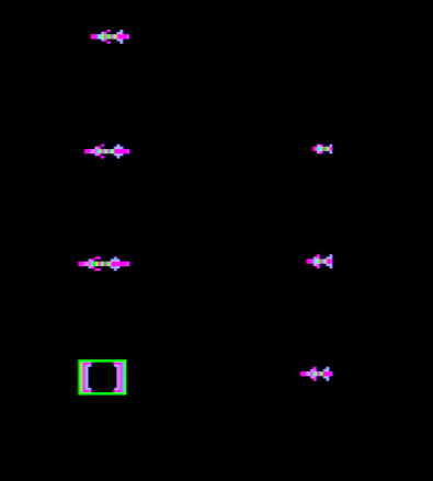
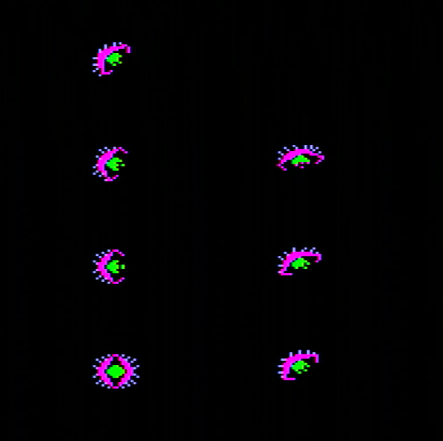
And then looking again at the Sprites in the Graphics ROM...
So that's all working just fine and dandy!
NivagSwerdna2022-03-27 10:56:28
Galaxian does not switch banks, however Moon Cresta requires extra addressing to cover the larger (2532 Graphics ROMs); to facilitate this the driver latch at 6000 is re-purposed from 1P Start LED, 2P Start LED and Coin Lockout to 3 bits of bank switching data. The driver latch 9M is also moved from 6000 to A000 in the memory map.
The upshot of this is that you effectively get 3 1-bit registers at A000, A001 and A002.
A002 is effectively "Bank Switch Enable", and A001 and A000 are bank number.
To accomplish this the bodge is as follows... An extra 74LS157 mux is mounted on 3J and a 74LS10 triple input NAND on top of 3M.
The extra inputs from 9M are routed via wires that cross the board.
The upshot of this is when A002 is 0 the original Galaxian scheme is followed but when A002 is 1 then A9 is driven by latch A000 and A10 is driven by latch A001. (Actually not all of the address space... the triple input NAND is used to stop some sprite remapping)
Anyway... we can see the effect by setting up some Sprites...
With A000..2 set to 000... i.e. no remap
Sprites 20, 21, 22, 23, 24, 25, 26 (hex)...
then changing the banking...
With A000..2 set to 100... i.e. remap, bank 00
With A000..2 set to 101... i.e. remap, bank 01
With A000..2 set to 110... i.e. remap, bank 10
With A000..2 set to 111... i.e. remap, bank 11
And then looking again at the Sprites in the Graphics ROM...
So that's all working just fine and dandy!
NivagSwerdna2022-03-27 10:56:28