First fix frogger on galaxian bootleg

drbible

User
vacBacker
Feedback
2 (100%)
Credits
98CR
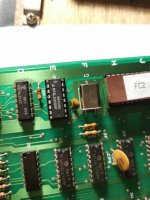
Now replaced the quartz and the 74368 as well as put in new sockets for that and the EPROMs.
Got 2 basic questions now if anyone has the patience to help further:
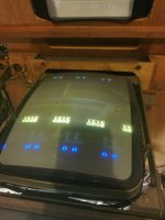
Signals are different now but what should a 6mhz clock signal appear like on a logic probe. I don't have an oscilloscope.
How do you check a capacitor like the one at c32? This is the last bit at the clock source that I haven't replaced. I could maybe source one from somewhere and replace it anyway.
 

Attachments

  • 16802852504558540570326114056892.jpg
    16802852504558540570326114056892.jpg
    79 KB · Views: 22

cliff_poole

Active member
vacBacker
Feedback
6 (100%)
Credits
1,069CR
Brilliant !, thanks for the link.

I've got a load of 80's hacked bootleg PCBs. Many years ago I decided, once I already had a working Galaxian and Scramble, I might as well leave the old hacks as they are. My interest has recently been renewed after reading the Arcade Britannia book. Some even have the converter's sticker on them, I'd previously not taken any notice of these, now I know a bit more about their history.
 

NivagSwerdna

Active member
Feedback
1 (100%)
Credits
744CR
OK... in an attempt to be more helpful.... Replace the XTAL with the original. You notice it is 18.432MHz. The original crystal should play nicely with the small capacitor and the pair of resistors around it. I'm 99.999% sure those parts are fine. In your original pictures there was a screen full of stuff... that suggested that at that time most of the timing circuits were working.

So... replace the XTAL. Then for the device at 1E measure the voltage between pins 8 and pins 16. Then with your logic probe go around all 16 pins and then report back.
 

drbible

User
vacBacker
Feedback
2 (100%)
Credits
98CR
OK... in an attempt to be more helpful.... Replace the XTAL with the original. You notice it is 18.432MHz. The original crystal should play nicely with the small capacitor and the pair of resistors around it. I'm 99.999% sure those parts are fine. In your original pictures there was a screen full of stuff... that suggested that at that time most of the timing circuits were working.

So... replace the XTAL. Then for the device at 1E measure the voltage between pins 8 and pins 16. Then with your logic probe go around all 16 pins and then report back.
You're right I'm taking a scattergun approach at best! Thanks for hanging in there Have upskilled my soldering and desoldering that's for sure. Slower progress on the understanding of the schematics etc.
Anyway, made some progress.....did what you said and the voltage is clean 5v. 1E Pin logic probe readings are: Lo,Lo(diff tone),Nil,Nil,Lo,Nil,Nil,Lo,Nil,Lo(diff tone),Nil,Lo(diff tone),Hi,Lo,Lo,Hi.

That aside the pic is better now so you're right the timing isn't all bad. I was testing the reset circuit and noticed without the ROM board it worked. I replaced the sockets the ROM board goes into. Also I removed the ROMs on there and discovered this horror (see pic)! Dried it out and now better.
Interestingly it also only got better when I removed the solder from the the pins I had repaired too so I guess that confirms they were snipped on purpose as part of the conversion although still not sure about this.
I'm guessing the next thing is to check out if the ROM chips are actually OK. What I haven't done is replace the IC sockets on the ROM board as the soldering is more intricate with tightly packed traces on there.
 

Attachments

  • IMG_20230401_185828.jpg
    IMG_20230401_185828.jpg
    115.6 KB · Views: 15
  • IMG_20230402_195535.jpg
    IMG_20230402_195535.jpg
    48.9 KB · Views: 16
  • IMG_20230402_195446.jpg
    IMG_20230402_195446.jpg
    52.9 KB · Views: 13
  • IMG_20230402_195449.jpg
    IMG_20230402_195449.jpg
    53.2 KB · Views: 12

drbible

User
vacBacker
Feedback
2 (100%)
Credits
98CR
Here are the instructions for the conversion, check that the tracks you repaired really needed to be repaired...
Item 4 is hard to read but this is ic 2N
Just read this properly - spot on thx. One of the IC legs I repaired was supposed to be snipped.
 

drbible

User
vacBacker
Feedback
2 (100%)
Credits
98CR
Which probe did you get? On mine... https://www.elenco.com/wp-content/uploads/2017/10/LP560-3.pdf it is very clear what is a pulse.
Obviously all the clocks are working to get an image like that.

This is what I would expect
View attachment 2667
Mine was from Halfords 😬. It does pulse for example at the reset pins without ROMs installed but I guess that's different as it's a simple voltage hi lo pulse. It just doesn't seem to recognise the clock pulse although the signal does sound different (scratchy) so you can kind of tell. I'm left wanting for a digi oscilloscope but that's a next level commitment.
Anyway had a thought I can presumably just try my original frogger ROMs on the board - will dig out the PCB and look.
 

drbible

User
vacBacker
Feedback
2 (100%)
Credits
98CR
Should get time to look at this next week. Question: is it worth doing anything I.e. checking address lines etc without getting all the ROMs on the bootleg ROM board checked out first? 20230413_193232.jpg
 

NivagSwerdna

Active member
Feedback
1 (100%)
Credits
744CR
It seems it came my way....

Before

2023-04-21_19-58-58.png
Rather Slimy... seems to be covered in an oil mist?

Nice looking ROMs...

1682104120836.png

DURING

All ROM checksums match the expected frogg...
Code:
ROM_START( frogg )
    ROM_REGION( 0x10000, "maincpu", 0 )
    ROM_LOAD( "p1.bin",       0x0000, 0x0800, CRC(1762b266) SHA1(2cf34dcfe00dc476b327f9d762a8d2aa268a2d25) )
    ROM_LOAD( "p2.bin",       0x0800, 0x0800, CRC(322f3916) SHA1(9236aaa260c4db4adbd92c8bba3674d07d7235a8) )
    ROM_LOAD( "p3.bin",       0x1000, 0x0800, CRC(28bd6151) SHA1(1a5bc540168fa5fef01bd7bc2cdbdb910c9a4ba4) )
    ROM_LOAD( "p4.bin",       0x1800, 0x0800, CRC(5a69ab18) SHA1(40b7bf200f87e0fb3fb54726ba79387889446052) )
    ROM_LOAD( "p5.bin",       0x2000, 0x0800, CRC(b4f17745) SHA1(2f237a667f6c95af213b787620142c1530d3cdd8) )
    ROM_LOAD( "p6.bin",       0x2800, 0x0800, CRC(34be71b5) SHA1(3088fc5817a397d0a87610d62845c7b8c4440f57) )
    ROM_LOAD( "p7.bin",       0x3000, 0x0800, CRC(de3edc8c) SHA1(634d54fb19b422b56576a196bdaf95733c52c7ee) )

Relabelled and also read through the sockets...

Code:
b5556ea939f02551b3d1962afc207e2c82ce4c82  0000-1FFF
c30644e75cf05285cd22e8f63cfe1e39cd9983f1  2000-37FF

All good!


AFTER

2023-04-21_20-07-06.png

On it's way back to its owner.

PS

You can read the sockets as 2532s but need to parallel the select pins as they aren't wired on the board itself (and also disable the side you are not reading)... something like this...

IMG_20230421_193056351.jpg
 
Last edited:

drbible

User
vacBacker
Feedback
2 (100%)
Credits
98CR
Right, finally got this onto a bench and all wired up. Couple (more) basic questions if I may:
I presume clock is fine as I'm getting a moving picture just garbled graphics. However clock signals don't show up as at all correct using my logic probe - don't get this?
Also can I check the address lines without the ROM board attached as some of the RAM chips are hidden below it so can't access them easily?
Lastly - using a galaxian schematic once the address and data lines reach a ROM chip how do I know which one of these frogger ICs are the ones to check instead?
Prime suspect for me right now is video RAM lines but that's a fairly randomly generated statement.
Wondering about an oscilloscope investment but trying to resist.
 

NivagSwerdna

Active member
Feedback
1 (100%)
Credits
744CR
You should be able to get quite a long way with just your logic probe. Make sure it has a nice positive and negative supply... does it go high when on pin 14 of things and low when on pin 7 of things?

Can you post a picture/video of what the screen is showing?
 

drbible

User
vacBacker
Feedback
2 (100%)
Credits
98CR
Can't seem to post videos but the screen moves like the frogger game or like the high score table.
Probe has solid high on 5v and lo on GND. Pins 7 and 14 of CPU or EPROM show active data i.e. both hi lo signals lit.
Can't get any clock signals to show correct. Reset looks OK on high although the lo on power up is hard to notice. It's momentary at best. Not sure how to force a reset on this board.
 

ArcadePCB

User
vacBacker
Credits
509CR
Without a ROM its difficult to test the system, because no program is executed. But you can remove the ROMs and tie all the data lines (D0..D7) to ground (use resistors 220 Ohms to 470 Ohms to limit the current for unexpected circumstances). This causes the Z80 to execute NOP instructions at every single address. So you can check the address lines: A15 has the lowest frequency, A14 is twice the frequency of A15, A13 is twice the frequency of A14 and so on. So using an oscilloscope can at least help to detect abnormal address lines (high level OK / low level OK / waveform OK / frequency OK, ...). If there is a stuck at low or a stuck at high or an undesired connection between two address lines, you wil see it on the scope. Just using a logic probe may in some situations help to find faults, but it's of course not able to replace an oscilloscope.
If the address bus is fine, you'll need the ROM to test further issues.

The repeated graphics on your pictures could be a sign of an addressing issue (wrong ROM is selected). Check the chip select signals of all ROMs / RAMs first. If any of it is permanently selected (low) or deselected (high), it's suspect. In this case, have a look at the address decoding circuits.

But that's just a guess from the far, you have to measure what's going on on the board.
 

NivagSwerdna

Active member
Feedback
1 (100%)
Credits
744CR
Does it play? e.g. coin up and then things move?

The graphics and the game play should be relatively independent. If it plays then you know half of it works.

I'm not familiar with frogg so cannot really infer too much.
 
Top