You are using an out of date browser. It may not display this or other websites correctly.
You should upgrade or use an alternative browser.
You should upgrade or use an alternative browser.
Arduino In-Circuit Tester: Build Project
- Thread starter Judder
- Start date
Sorry didn't get round to committing any code, but I've made great progress tonight.
Still no DRAM tests but I have the interrupts working, 2 custom sound tests and I have the PIA setups and LCD under control.
Now I just need to figure out how to make the DRAM work
Still no DRAM tests but I have the interrupts working, 2 custom sound tests and I have the PIA setups and LCD under control.
Now I just need to figure out how to make the DRAM work
Is the DRAM completely inoperable, as in the RAM Write-Read test doesn't return anything like the write pattern?
The DRAM has RAS/CAS maximums of 10uS that may be tough to hit without a lot of optimizations. If you are able to measure the results of RAS/CAS with a scope and confirm the pulse length it may help point us in the right direction (versus some other specific bug in the implementation).
Paul.
The DRAM has RAS/CAS maximums of 10uS that may be tough to hit without a lot of optimizations. If you are able to measure the results of RAS/CAS with a scope and confirm the pulse length it may help point us in the right direction (versus some other specific bug in the implementation).
Paul.
PaulSwan said:Is the DRAM completely inoperable, as in the RAM Write-Read test doesn't return anything like the write pattern?
The DRAM has RAS/CAS maximums of 10uS that may be tough to hit without a lot of optimizations. If you are able to measure the results of RAS/CAS with a scope and confirm the pulse length it may help point us in the right direction (versus some other specific bug in the implementation).
I'll check on that over the weekend ...
Dave2084 said:For this little project the last bit is interrupts.
I need to get this to work as the sound inputs drive the PIA CB1 to generate an IRQ to the 6802. This needs testing to ensure it all works properly (the 4068 at IC6 that feeds CB1 is a common fail).
Hi Dave
Is the Interrupt Check test working at the moment BTW?
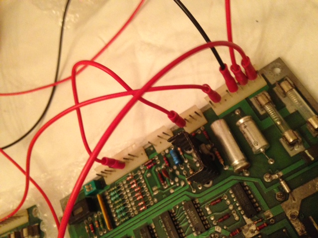
Just testing a Defender Sounds Board here, and everything passes fine except for this which just gives "E: Timeout", but I think that was the same for the other boards I tested
Also is the "Input Read" test checking IOJ3 Sound Select input (CB2, PB0, PB1 etc.)?
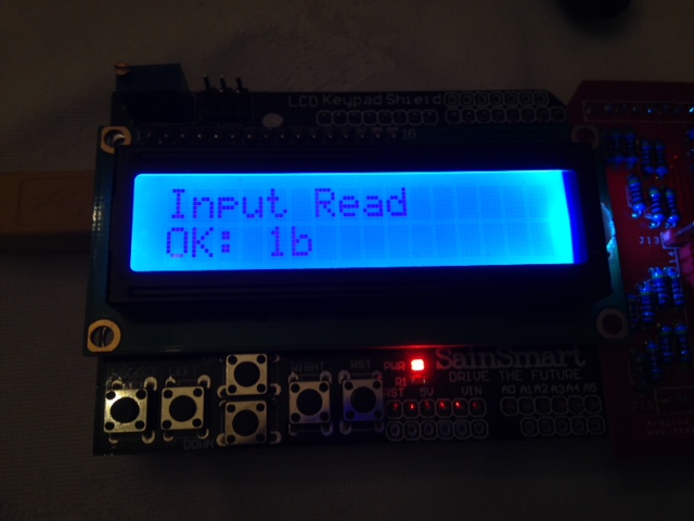
Input Read test is giving
U10 ff PB0-7 = 1f
but not totally sure how to interpret the results!
Regards
Alex
Judder said:Also is the "Input Read" test checking IOJ3 Sound Select input (CB2, PB0, PB1 etc.)?
Input Read test is giving
U10 ff PB0-7 = 1f
but not totally sure how to interpret the results!
Actually answering my own question, the result of the test can be deduced from the table in CwmsSoundBaseGame.cpp
Grounding pin 5 = 11111011
x, PB7, PB4, PB5, PB2, PB3, PB0, PB1
as pin 1 isn't connected, so the result should be 1b, which it is
Judder2016-02-20 23:04:38
Judder said:Dave2084 said:For this little project the last bit is interrupts.
I need to get this to work as the sound inputs drive the PIA CB1 to generate an IRQ to the 6802. This needs testing to ensure it all works properly (the 4068 at IC6 that feeds CB1 is a common fail).
Is the Interrupt Check test working at the moment BTW?
Just testing a Defender Sounds Board here, and everything passes fine except for this which just gives "E: Timeout", but I think that was the same for the other boards I tested
To run the interrupt test to completion you need to start the test, then ground one of the sound inputs before the timeout period ends (2.5 seconds, maybe I should make this longer?).
I did add some comments to the source code but maybe it needs more:
Code:
//

// This is used to test /IRQ: 6802 CPU U9 Pin 4 is pulled low by 6821 PIA U10 /IRQA Pin 37 or /IRQB Pin 38

// This is triggered by 6821 PIA U10 CB1 Pin 18 being pulled high when a sound input is triggered through 4068 U6

//
Judder said:Also is the "Input Read" test checking IOJ3 Sound Select input (CB2, PB0, PB1 etc.)?
Input Read test is giving
U10 ff PB0-7 = 1f
but not totally sure how to interpret the results!
More source code comments:
Code:
//

// Input region - IC10 6821 PIA Inputs from ROM board (PB0-7)

//

// Sound board Inputs on 0x4000

//       4J3-1 - Key                                         0x01  PB0 - 4J3-3

// 0x02  4J3-2 - PB1                                         0x02  PB1 - 4J3-2

// 0x01  4J3-3 - PB0                                         0x04  PB2 - 4J3-5

// 0x08  4J3-4 - PB3                                         0x08  PB3 - 4J3-4

// 0x04  4J3-5 - PB2                                         0x10  PB4 - 4J3-7

// 0x20  4J3-6 - PB5 (W4 Installed & W9 Removed)             0x20  PB5 - 4J3-6 (W4) / DSW-2 (W9)

// 0x10  4J3-7 - PB4                                         0x40  PB6 - DSW-1

// 0x80  4J3-8 - PB7 (W12 Installed)                         0x80  PB7 - 4J3-8 (W12)

//       4J3-9 - No Connection

//

// 0x40  DSW-1 - PB6

// 0x20  DSW-2 - PB5 (W4 Removed & W9 Installed)

//
Arv said:Would you be able to test Williams system 3-7 boards with this?
Obviously with a bit coding like?
Yes!
These are all very similar to the Williams sound boards but with much more IO.
System 6+7 would be trivial to do as they also use 6802
System 3+4 would need more effort as they use 6800 and will probably need clock mastering.
Bally 6800 boards could also be implemented.
These are all on my todo list.
Dave2084 said:I did add some comments to the source code but maybe it needs more:
Code:// // This is used to test /IRQ: 6802 CPU U9 Pin 4 is pulled low by 6821 PIA U10 /IRQA Pin 37 or /IRQB Pin 38 // This is triggered by 6821 PIA U10 CB1 Pin 18 being pulled high when a sound input is triggered through 4068 U6 //
I'd probably add a little comment highlighting the grounding of an active PIA pin in the 1.5 second window to test.
It works great BTW

Judder said:Also is the "Input Read" test checking IOJ3 Sound Select input (CB2, PB0, PB1 etc.)?
Also works great and testing on a Defender I get
9 8 7 6 5 4 3 2 1
N/C CB2 PB4 PB5 PB2 PB3 PB0 PB1 x
0 0 0 1 1 1 1 1 = 0x0f
0 0 1 0 1 1 1 1 = 0x1f
0 0 1 1 0 1 1 1 = 0x1b
0 0 1 1 1 0 1 1 = 0x17
0 0 1 1 1 1 0 1 = 0x1e
0 0 1 1 1 1 1 0 = 0x1d
which is correct as if we put them in binary sequence
PB5 PB4 PB3 PB2 PB1 PB0
0 1 1 1 1 1 = 0x1f
0 0 1 1 1 1 = 0x0f
0 1 0 1 1 1 = 0x17
0 1 1 0 1 1 = 0x1b
0 1 1 1 0 1 = 0x1d
0 1 1 1 1 0 = 0x1e
Also the DAC test works great - here's a slightly amended array which produces a chromatically scaling test - a bit more dog / lounge friendly

[font="Courier New, Courier, mono"] byte loops[] = { 80, 70, 60, 50, 40, 30, }; // how many times the waveform is repeated max=255[/font]
[font="Courier New, Courier, mono"] byte delay[] = { 50, 40, 30, 20, 10, 00, }; // how long each data value is left on the DAC max=255[/font]
[font="Courier New, Courier, mono"] byte waveform[] = { 0, 0, 0, 0, 0, 0, }; // waveform shape 0=Sine 1=Sawtooth 2=Square[/font]
Spent ages working on the ROM board IRQ as it wasn't checking the bit set to identify which of the 4 possible interrupts were triggered.
Ideally I wanted to be able to test them in any order but the code got convoluted and as we are running much slower issues would arise if two arrived in the same read cycle so I've gone back checking then in the order CA1, CA2, CB1, CB2 with only one at a time enabled. It's not really too bad as long as you know that two of them need to be grounded at the appropriate time, I've given a 5 second window for this.
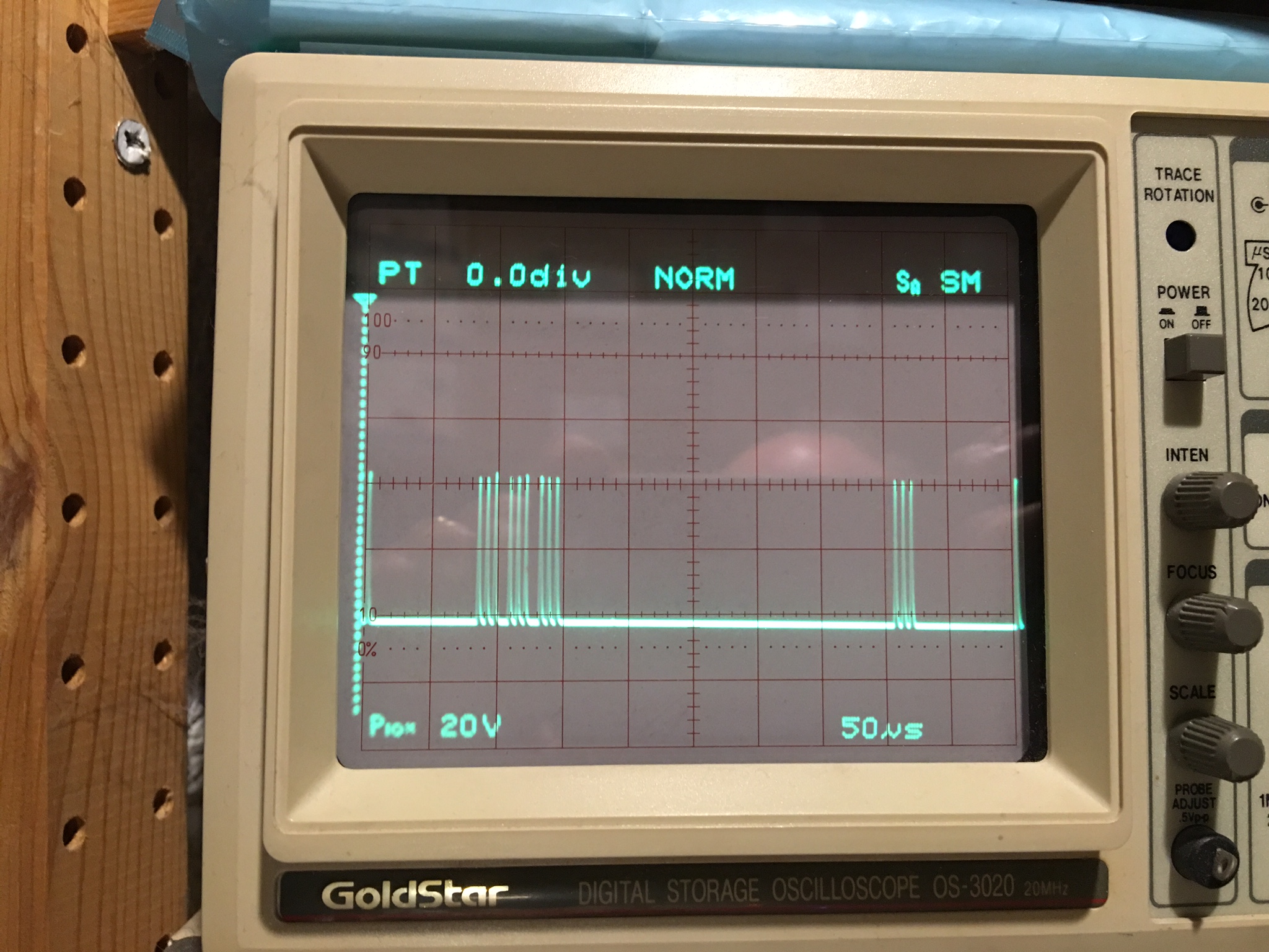
Looking at the /CAS and /RAS timing for the DRAM we're around 0.4ms which is just too slow, it also doesn't help that the clock pulses are bursted rather than constant. In fact looking at the photos below again now it seems they are both following the clock (note the scales are slightly different here). I'll have to examine some more ...
/CAS and /RAS at 100uS/Div
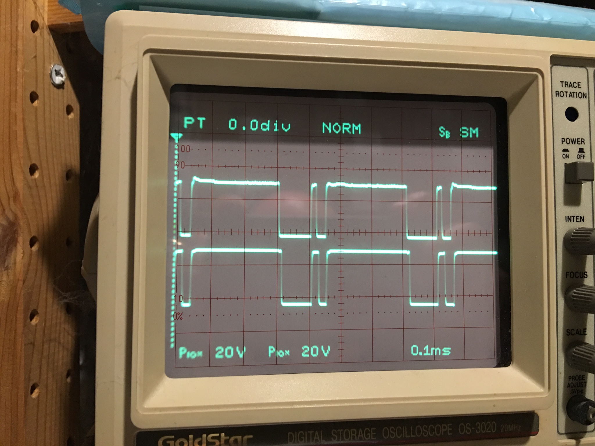
Clock Pulses at 50uS/Div
Dave20842016-02-21 19:21:10
Ideally I wanted to be able to test them in any order but the code got convoluted and as we are running much slower issues would arise if two arrived in the same read cycle so I've gone back checking then in the order CA1, CA2, CB1, CB2 with only one at a time enabled. It's not really too bad as long as you know that two of them need to be grounded at the appropriate time, I've given a 5 second window for this.
Looking at the /CAS and /RAS timing for the DRAM we're around 0.4ms which is just too slow, it also doesn't help that the clock pulses are bursted rather than constant. In fact looking at the photos below again now it seems they are both following the clock (note the scales are slightly different here). I'll have to examine some more ...
/CAS and /RAS at 100uS/Div
Clock Pulses at 50uS/Div
Dave20842016-02-21 19:21:10
Judder said:I'd probably add a little comment highlighting the grounding of an active PIA pin in the 1.5 second window to test.
Already done on Github. I also increased the timeout window to 2.5 seconds. Might set it to match the ROM board interrupts of 5 seconds. What do you think?
Judder said:Also the DAC test works great - here's a slightly amended array which produces a chromatically scaling test - a bit more dog / lounge friendly
I'll try it out sometime.
PaulSwan said:I only have a corroded Defender main board that I'm hoping works enough to try out. LMK when you've pushed.
Pushed ...
https://github.com/Dave2084/arduino-mega-ict/tree/arduino-mega-ict-williams
It looks like the Defender main I have is too corroded to be viable to work with
Can you confirm what operation your scope traces represent? Read, write or write-read, for example?
I didn't do any optimizations for 6809 since Star Wars is static so there is some scope to optimize the bus cycles.
Paul.
PaulSwan2016-02-22 06:14:02
Can you confirm what operation your scope traces represent? Read, write or write-read, for example?
I didn't do any optimizations for 6809 since Star Wars is static so there is some scope to optimize the bus cycles.
Paul.
PaulSwan2016-02-22 06:14:02
The RAM Write-Read option will write 11 22 33 44 and then just print the results from the read at the first 4 bytes of the memory block selected.
After reset, the setup options are available that includes the "Set Repeat" for rerunning the same test for a few seconds and "Set Error" to ignore errors and keep repeating the test.
It would be useful to see a trace of the master clock versus RAS. If you are doing only reads then the long & short RAS traces seem unexpected. If anyone has a spare Defender board they're willing to send me I can take a look myself also.
Paul.
I tested out the clock master version of 6502 on Astro Fighter this morning and it worked OK. There is 16Kb of 4116 on this platform as well. In test, I got a consistent single bit error in the RAM test of the DRAM. Splitting the block into two halves was enough to get a consistent DRAM test pass on this platform with ITT 4027 DRAM.
The DRAM timing logic is probably the most complicated bus cycle in most platforms, especially since it's often shared with video access, so given that I suspect in the Defender case there is a bug in the 6809 implementation or special accommodation needed for Defender specifically (I needed one for 6502 on Astro Fighter). I'll see if I can deduce the DRAM cycle to see where the problem is.
Paul.
PaulSwan said:I tested out the clock master version of 6502 on Astro Fighter this morning and it worked OK. There is 16Kb of 4116 on this platform as well. In test, I got a consistent single bit error in the RAM test of the DRAM. Splitting the block into two halves was enough to get a consistent DRAM test pass on this platform with ITT 4027 DRAM.
The DRAM timing logic is probably the most complicated bus cycle in most platforms, especially since it's often shared with video access, so given that I suspect in the Defender case there is a bug in the 6809 implementation or special accommodation needed for Defender specifically (I needed one for 6502 on Astro Fighter). I'll see if I can deduce the DRAM cycle to see where the problem is.
This might be useful:
http://www.robotron-2084.co.uk/manuals/defender/defender_early_pcb_theory.pdf
I was hoping to have a look this evening and see what is happening but ran out of time ... soon!
Thanks for that, saved a lot of time. Basically, it needs a similar accommodation to what was needed in 6502 to delay reading the data to the very end of the cycle due to synchronous external logic.
I've updated 6809E to add such support along with interrupt locks to improve determinism and moving the D write into the idle phase to shorten the RAS/CAS active pulse times for writes.
https://github.com/prswan/arduino-mega-ict/tree/6809e
From the timing diagram in that doc, it looks like the QLo to D read delay should be 3 clock pulses (the RAS Hi latching the data after QLo seems to be the reason data read after QLo didn't return any DRAM data).
Paul.
PaulSwan2016-02-25 06:18:33